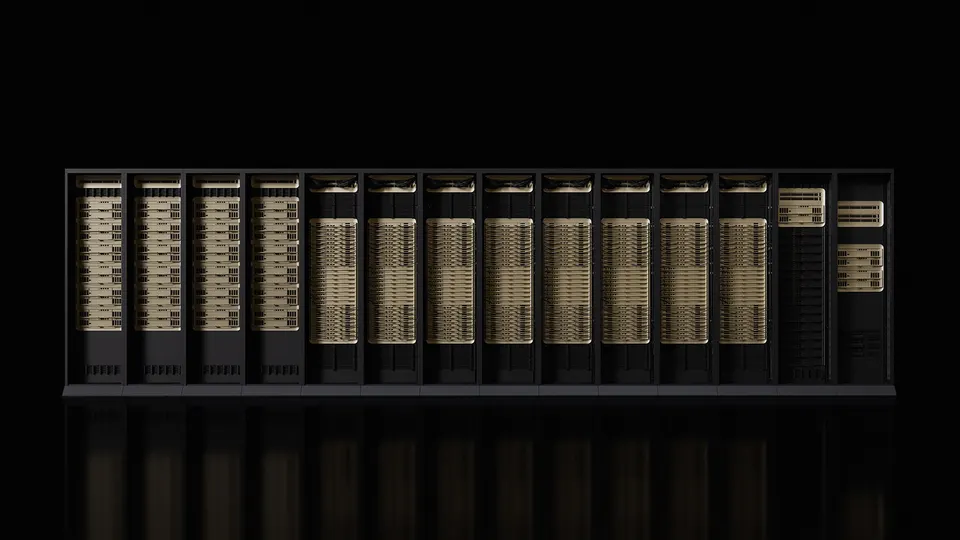

Milestones
- Rubin named on roadmap at ComputexJun 2024Complete.
- Vera Rubin detailed at GTC for H2 202618 Mar 2025Complete.
- Full platform unveiled at CESJan 2026Complete.
- Volume productionJun 2026Complete.
- Partner cloud shipmentsTarget Q4 2026Current milestone.
- Rubin Ultra (NVL576 Kyber rack)Target 2027Not yet reached.
- Feynman architectureTarget 2028Not yet reached.
Most important updates
- 16d ago
- 6 Jul 2026
- 31 May 2026
- Jan 2026
- 18 Mar 2025
Upcoming
- Q4 2026Partner cloud shipments (next)
- Q4 2026Vera Rubin availability at major clouds
- 2027Rubin Ultra (NVL576 Kyber rack)
- 14 Mar 2027GTC 2027 roadmap update (Rubin Ultra, Feynman)
- 2028Feynman architecture
Current obstacles
- HBM4 and CoWoS supplyOutput is limited by HBM4 memory supply and TSMC's packaging capacity, not only by GPU chips.
- Rack power deliveryFuture racks head toward hundreds of kilowatts, forcing new 800 V power and cooling designs.
Physics limits
- The memory wallArithmetic per chip has grown far faster than memory speed. Writing each token means re-reading the model's weights from HBM, so much of the time the GPU waits on memory, not maths.
- A single die can't exceed about 858 mm²Scanners expose at most 26 × 33 mm per shot, so no one chip can be larger. Bigger GPUs must join several dies, paying energy and delay at every seam between them.
- Heat densityA 72-GPU rack draws well over 100 kW, roughly ten times an older server rack, and all of it becomes heat. Air can't remove it; liquid cold plates are nearing how much heat they can pull from each square centimetre.
How it works
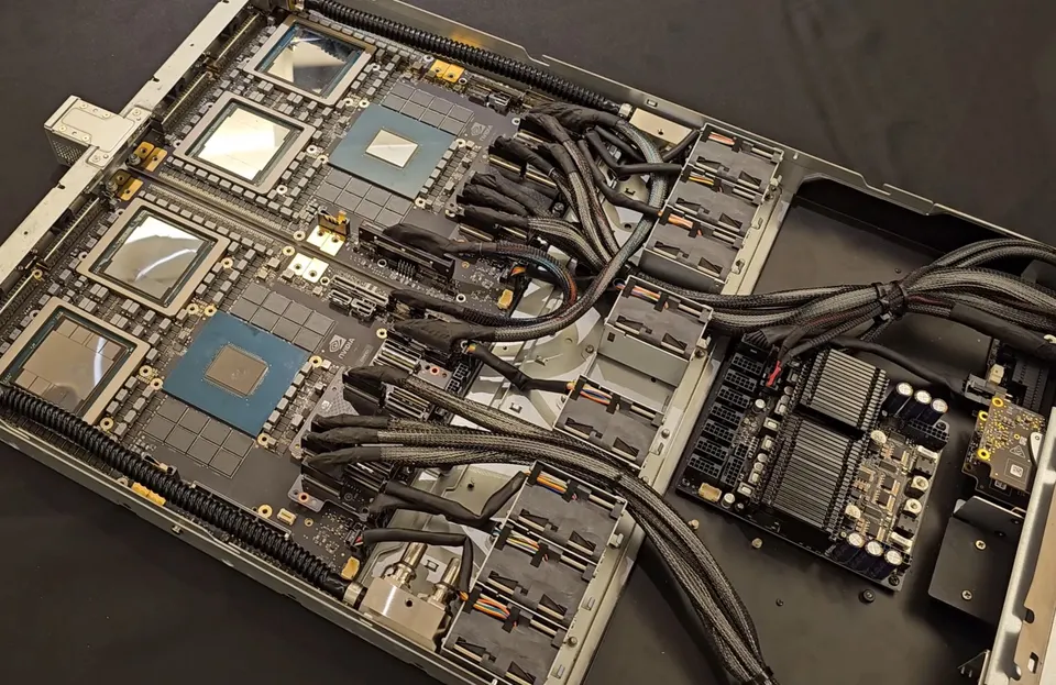
Package
Two dies act as one GPU
Each Rubin joins two maximum-size chips with a fast link and surrounds them with HBM4 memory stacks.
Memory
HBM4
HBM4 doubles the memory connection width, giving about 22 TB/s per GPU. That speeds up inference.
Precision
NVFP4
A 4-bit number format keeps accuracy close to 8-bit while doing twice the work per second.
Rack
NVLink 6 spine
72 GPUs and 36 CPUs share one switch network, so the liquid-cooled rack acts like one big chip.
Spec sheet
| Spec | Vera Rubin | Blackwell Ultra (GB300) | Change |
|---|---|---|---|
| GPU transistors | 336 billionR (reported) | 208 billion (Blackwell) | ▲ 128 billion |
| Process | TSMC 3 nm classR (reported) | TSMC 4NP | —no comparable change |
| NVFP4 inference per GPU | 50 PFLOPSR (reported) | — | —no comparable change |
| NVFP4 training per GPU | 35 PFLOPSR (reported) | — | —no comparable change |
| HBM per GPU | 288 GB HBM4R (reported) | 288 GB HBM3e | —no comparable change |
| Memory bandwidth per GPU | 22 TB/sR (reported) | 8 TB/s | ▲ 14 TB/s |
| NVL72 rack NVFP4 inference | 3.6 exaflopsR (reported) | — | —no comparable change |
| NVL72 rack HBM4 | 20.7 TBR (reported) | — | —no comparable change |
| Vera CPU cores | 88 custom Arm coresR (reported) | 72 (Grace) | —no comparable change |
R reported by the company
Update log
Thu 24 Sep
- Minor: PressCommercial
Mon 6 Jul
- Minor: PressManufacturing
Sun 31 May
- Major: PressManufacturing
Jan 2026
- Major: PressHardware
Tue 9 Sep 2025
- Minor: PressHardware
Tue 18 Mar 2025
- Major: BlogHardware
About NVIDIA
NVIDIA
AI GPUs, rack systems, CUDA, networking
NVIDIA designs the GPUs, networking and software behind most AI training and inference. Its CUDA software made GPUs the default for AI. In October 2025 it became the first company worth $5 trillion.
- Vera Rubin in production in 2026; cloud partners get it from the second half of the year.
- Licensed Groq's inference technology and hired its leaders for about $20B (Dec 2025).
- Plans to invest up to $100B in OpenAI, tied to at least 10 GW of NVIDIA systems (Sep 2025).
- Founded
- 199333 yrs
- Headquarters
- United States
- Status
- Public
- Listed
- NVDA (opens google.com)NASDAQ
- Valuation
- $5.4Tmarket capSep 2026
- Staff
- ~36,000Jan 2025
- Coverage
- 3 programs · 21 updateslatest 16d agochecked 25 Sep
- People
- Jensen Huang (opens en.wikipedia.org)Co-founder, President and CEOColette Kress (opens en.wikipedia.org)CFOBill Dally (opens en.wikipedia.org)Chief Scientist