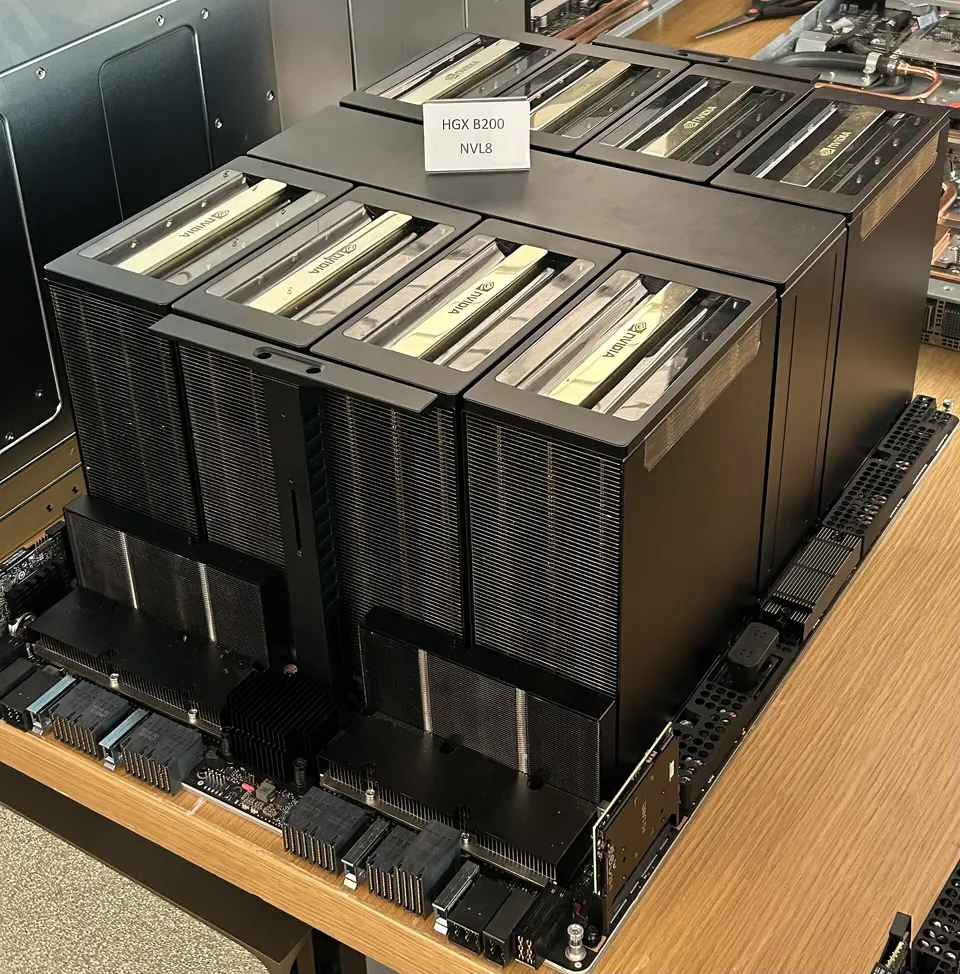

Milestones
- Blackwell announced at GTC18 Mar 2024Complete.
- Mask change to fix yield issue delays rampAug 2024Complete.
- GB200 NVL72 racks ship to customersQ4 2024Complete.
- Blackwell Ultra (GB300) announced18 Mar 2025Complete.
- GB300 NVL72 shippingQ3 2025Complete.
Most important updates
- 9 Oct 2025
- 3 Jul 2025
- 4 Jun 2025
- 26 Feb 2025
- 18 Mar 2024
Current obstacles
- Rack-scale integrationEarly GB200 racks overheated and had connection issues. Shipping 120 kW liquid-cooled racks is hard.
Physics limits
- Copper reaches only about a metre at top speedAt about 200 Gb/s per wire pair, electrical signals fade within roughly a metre of copper. That confines NVLink's all-to-all domain to one rack; going further needs optics, which cost power.
- Number formats can't shrink much furtherGoing from 16 to 8 to 4 bits roughly doubled throughput each step. Below about 4 bits, numbers can't represent weights and activations accurately enough, so this lever is nearly used up.
- Each die is already at the size limitEach Blackwell die is close to the 26 × 33 mm maximum a scanner can print. Growth now means joining dies, and the link between them costs chip area and energy for every bit that crosses it.
How it works
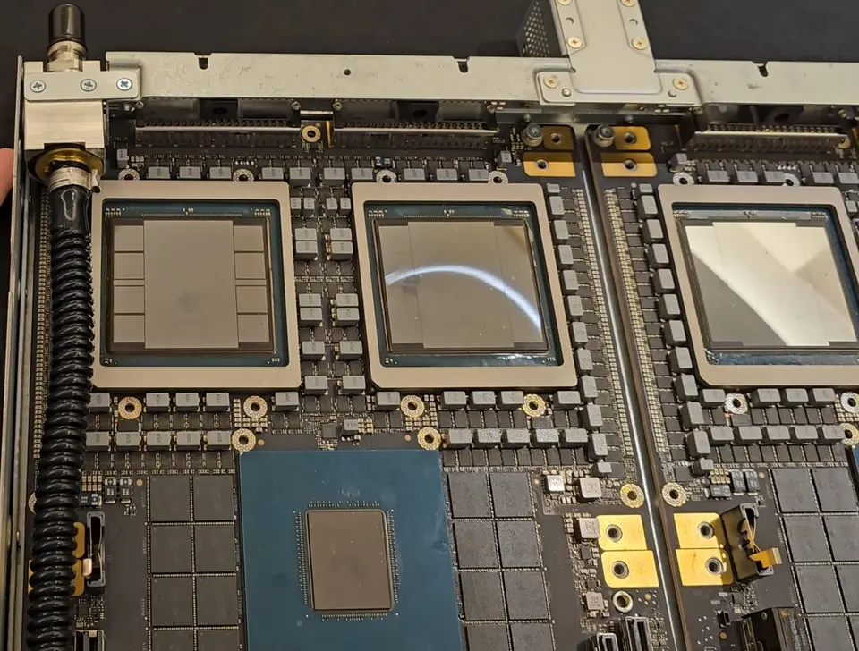
Dies
Two dies act as one GPU
Two maximum-size dies (208 billion transistors in total) are joined by a 10 TB/s link, so software sees a single GPU.
Memory
HBM3e beside the dies
Eight HBM3e stacks give 192 GB (B200) or 288 GB (B300) at about 8 TB/s, so a large model fits on fewer GPUs.
Precision
4-bit maths where it's safe
The Transformer Engine picks 4-, 6- or 8-bit number formats per block of values, doubling throughput over 8-bit when accuracy allows.
Rack
NVL72
72 GPUs and 36 Grace CPUs are linked by NVLink switches at 1.8 TB/s per GPU, in one liquid-cooled rack of roughly 120 kW.
Update log
Thu 9 Oct 2025
- Major: BlogCommercial
Thu 3 Jul 2025
- Minor: PressCommercial
Wed 4 Jun 2025
- Minor: BlogTest
Wed 26 Feb 2025
- Major: PressCommercial
Mon 18 Mar 2024
- Major: PressHardware
About NVIDIA
NVIDIA
AI GPUs, rack systems, CUDA, networking
NVIDIA designs the GPUs, networking and software behind most AI training and inference. Its CUDA software made GPUs the default for AI. In October 2025 it became the first company worth $5 trillion.
- Vera Rubin in production in 2026; cloud partners get it from the second half of the year.
- Licensed Groq's inference technology and hired its leaders for about $20B (Dec 2025).
- Plans to invest up to $100B in OpenAI, tied to at least 10 GW of NVIDIA systems (Sep 2025).
- Founded
- 199333 yrs
- Headquarters
- United States
- Status
- Public
- Listed
- NVDA (opens google.com)NASDAQ
- Valuation
- $5.4Tmarket capSep 2026
- Staff
- ~36,000Jan 2025
- Coverage
- 3 programs · 23 updateslatest 2d agochecked 25 Sep
- People
- Jensen Huang (opens en.wikipedia.org)Co-founder, President and CEOColette Kress (opens en.wikipedia.org)CFOBill Dally (opens en.wikipedia.org)Chief Scientist