
The brief
- N2 (2 nm class) in volume production since Q4 2025. A16 is planned for the second half of 2026.
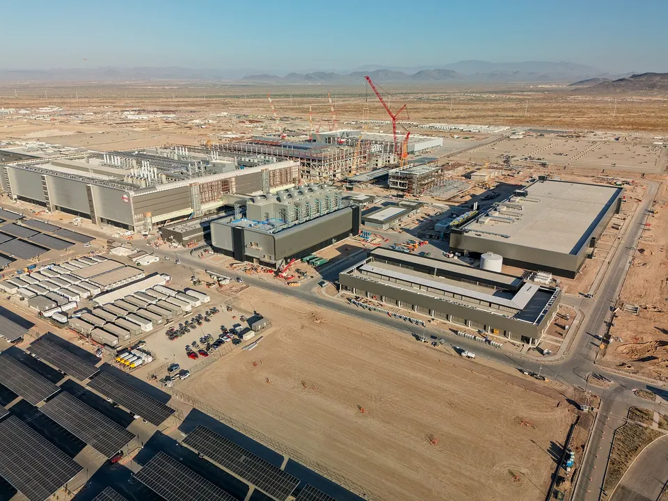
- Pledged $165B in total for US factories, packaging and R&D in Arizona.
- Makes nearly all leading AI chips and packages them with CoWoS.
Technical approach
Foundry-only model
TSMC sells no chips of its own, so rivals trust it with their designs. Many customers fund each new node.
Nanosheet gate-all-around
N2 swaps fin-shaped transistors for stacked silicon sheets wrapped by the gate. They leak less power.
Backside power (A16)
A16 moves power wiring under the transistors, leaving the top free for signal wires.
CoWoS and SoIC
CoWoS places processor chips and HBM memory side by side on a shared base. SoIC stacks chips directly.
TSMC, three programs
Updated 16 Jun 2026

Research & demos
- Apr 2025
Laid out the node after A16, targeted for 2028.
- Dec 2024
First detailed public data on how N2 transistors and memory cells perform.
- Apr 2024
Introduced TSMC's approach to putting power wiring under the transistors.
Open technical problems
- Rising cost per waferOpen
Each node needs more steps and EUV exposures, so wafers cost more and savings per transistor shrink.
- Geographic concentrationActive research
Most advanced capacity is in Taiwan. Building abroad is slower and costlier, with worker gaps.
- Packaging capacityActive research
Demand for CoWoS packaging has beaten supply for years despite fast expansion.
Upcoming catalysts
- 20279.5-reticle CoWoS enters volume productionCoWoS advanced packagingby ~15 mo
- 2027Fab 2 begins N3 volume productionTSMC Arizonaby ~15 mo
Peers
Company & funding
- Listed
- TSM (opens google.com)NYSE
- Staff
- ~83,825as of 2024
- HQ
- TW
- Founded
- 1987
- Website
- tsmc.com (opens tsmc.com)
Partners & customers
- Customer
Largest customer; typically first on each new node.
- Customer
GPUs and CoWoS packaging.
- Customer
CPUs, GPUs and chiplets.
- Supplier
EUV lithography tools.
- Partner
Up to $6.6B CHIPS Act grant for Arizona fabs.
People
- C.C. Wei (opens en.wikipedia.org)Chairman and CEO
- Morris Chang (opens en.wikipedia.org)Founder (retired)