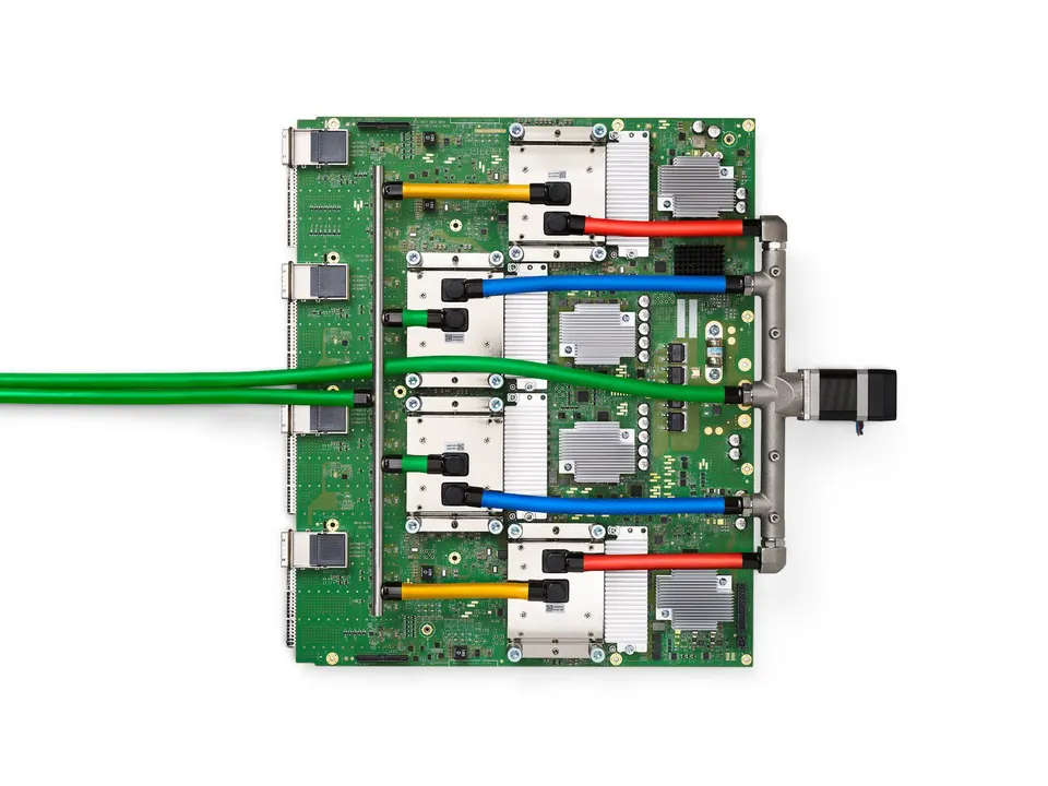

Milestones
- TPU v1 in production for inference2015Complete.
- TPU v4 pods with optical circuit switching2021Complete.
- Trillium (6th gen) announcedMay 2024Complete.
- Ironwood (7th gen) announced9 Apr 2025Complete.
- Ironwood generally availableNov 2025Complete.
- TPU 8t (training) and TPU 8i (inference) announced22 Apr 2026Complete.
- TPU 8t and TPU 8i generally availableTarget 2026Current milestone.
Most important updates
- 22 Apr 2026
- 6 Nov 2025
- 9 Apr 2025
- 14 May 2024
- 18 May 2016
Upcoming
- 2026TPU 8t and TPU 8i generally available (next)
- 2026TPU 8t and TPU 8i general availability, which Google said would come later in 2026
Current obstacles
- Software outside GoogleMost AI code is written for NVIDIA chips. Outside TPU users rely on Google's tools and improving PyTorch support.
Physics limits
- A chip can't be bigger than the reticleLithography prints at most about 26 x 33 mm (858 mm²) per exposure, so one die can't grow past that. Bigger systems need many chips and fast links between them.
- The memory wallChip arithmetic has grown far faster than memory bandwidth, so big models often wait on data. HBM helps, but each stack is limited by how many wires fit at its edge.
- Transistors are near atomic sizesAt 2 to 3 nm class nodes, key features are tens of atoms across. Leakage and tunnelling rise, and each new node brings smaller gains in speed and energy per operation.
How it works
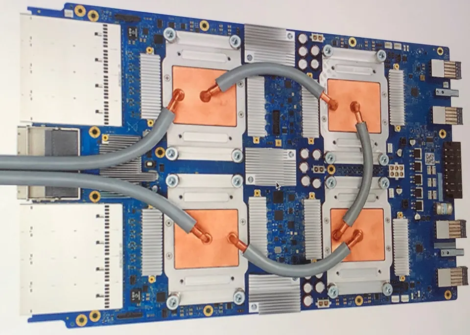
A grid that multiplies
Each core has systolic arrays: grids of thousands of multipliers that pass numbers to neighbours, doing matrix maths with little memory traffic.
High-bandwidth memory
Ironwood has 192 GB of stacked HBM per chip at about 7.4 TB/s, so large models stay close to the arithmetic units.
Thousands of chips as one
Chips link directly in a 3D torus; an Ironwood pod joins up to 9,216 chips, and optical switches can rewire a pod around failures.
Training and serving chips
The eighth generation splits into TPU 8t for training and TPU 8i for serving answers, with three times the on-chip memory for speed.
Spec sheet
| Spec | Tensor Processing Unit (TPU) |
|---|---|
| Peak compute per chip (FP8) | 4,614 TFLOPSR (reported) |
| HBM per chip | 192 GBR (reported) |
| HBM bandwidth | 7.37 TB/sR (reported) |
| Max chips per pod | 9,216R (reported) |
| Pod compute (FP8) | 42.5 exaflopsR (reported) |
R reported by the company
Update log
Wed 22 Apr
- Major: BlogHardware
Thu 6 Nov 2025
- Major: BlogHardware
Wed 9 Apr 2025
- Major: BlogHardware
Tue 14 May 2024
- Minor: BlogHardware
Wed 18 May 2016
- Major: BlogHardware
About Google DeepMind
Google DeepMind
Gemini, AlphaFold, Genie, Veo, TPU chips
Google DeepMind is Alphabet's AI lab, formed in 2023 from DeepMind and Google Brain. It builds the Gemini models and leads in AI for science. AlphaFold won a share of the 2024 Nobel Prize in Chemistry.
- Gemini 3 (Nov 2025) led many benchmarks. Gemini 3.5 Pro, announced in May 2026, is delayed.
- AlphaFold predicted structures for over 200 million proteins and won a share of the 2024 Chemistry Nobel.
- Google's own Ironwood TPU chip is used in-house and sold to outside labs, including Anthropic.
- Founded
- 201016 yrs
- Headquarters
- United KingdomUnited States
- Status
- Subsidiaryof Alphabet
- Valuation
- Alphabet-owned
- Coverage
- 5 programs · 30 updateslatest 29 Jul 2026checked 25 Sep
- Customers
- Anthropic
- Partners
- Isomorphic LabsBroadcom
- Acquired by
- Alphabet
- People
- Demis HassabisCEO and co-founderShane LeggCo-founder and Chief AGI ScientistJohn JumperAlphaFold lead; 2024 Nobel laureate