

Milestones
- N2 announced at Technology SymposiumJun 2022Complete.
- N3 volume production (previous node)29 Dec 2022Complete.
- N2 results presented at IEDMDec 2024Complete.
- N2 volume productionQ4 2025Complete.
- N2P and A16 volume productionTarget Q4 2026Current milestone.
- A14 productionTarget 2028Not yet reached.
Most important updates
- 27 Apr 2026
- Q4 2025
- 27 Aug 2025
- 24 Apr 2024
- 29 Dec 2022
Upcoming
- Q4 2026N2P and A16 volume production (next)
- 2028A14 production
Current obstacles
- GAA process controlThe stacked sheets need near-atomic precision. Small variations directly lower yield.
- Interconnect resistanceTiny copper wires resist current more as they shrink, eating into transistor gains.
Physics limits
- Electrons tunnel through barriers a few nanometres thickGates now control channels only a few nanometres long. At that scale electrons tunnel through barriers meant to stop them, so 'off' transistors leak and each new node brings smaller gains.
- Atoms are countableA nanosheet is about 5 nm thick, a few dozen atomic layers. One layer more or less, or a few misplaced atoms, shifts how a transistor behaves, so billions of identical transistors get harder to make.
- Thin wires resistCopper wires only tens of nanometres wide conduct worse, because electrons scatter off surfaces and grain boundaries and barrier liners take up space. Wiring delay and heat now limit chips as much as transistors do.
How it works
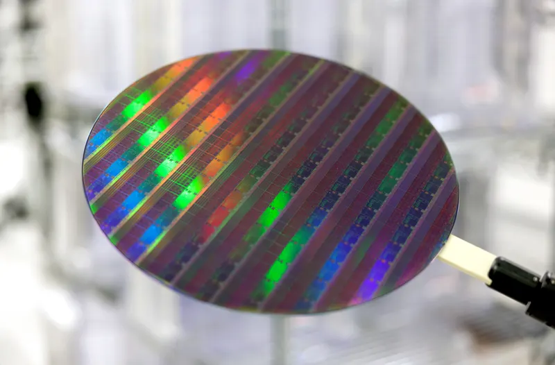
Nanosheets
Stacked horizontal channels
Current flows through thin silicon sheets stacked on top of each other. The gate wraps all 4 sides.
Patterning
EUV lithography
The finest layers are printed with EUV light from ASML machines, sometimes in several passes.
Cells
NanoFlex
Designers can mix small low-power cells and tall fast cells in one chip.
Spec sheet
| Spec | N2 process | N3E | Change |
|---|---|---|---|
| Transistor type | Nanosheet gate-all-aroundR (reported) | FinFET | —no comparable change |
| Speed at same power vs N3E | +10-15%R (reported) | — | —no comparable change |
| Power at same speed vs N3E | -25-30%R (reported) | — | —no comparable change |
| Chip density vs N3E | >1.15xR (reported) | — | —no comparable change |
| HD SRAM density | ~38 Mb/mm²R (reported) | — | —no comparable change |
| Wafer price | ~$30,000E (estimated) | — | —no comparable change |
R reported by the company · E our estimate
Papers & demos
- Dec 2024paper2nm platform technology featuring energy-efficient nanosheet transistors (IEDM 2024)First detailed public data on how N2 transistors and memory cells perform.
Update log
Mon 27 Apr
- Minor: PressOther
Q4 2025
- Major: OtherManufacturing
Wed 27 Aug 2025
- Minor: PressOther
Wed 24 Apr 2024
- Major: PressResearch
Thu 29 Dec 2022
- Major: PressManufacturing
About TSMC
TSMC
Chip foundry, N2, A16, CoWoS packaging
TSMC, founded in Taiwan in 1987, builds chips that other companies design. It makes most of the world's most advanced chips, including Apple's, NVIDIA's and AMD's. Its CoWoS packaging is a key bottleneck for AI chips.
- N2 (2 nm class) in volume production since Q4 2025. A16 is planned for the second half of 2026.
- Pledged $165B in total for US factories, packaging and R&D in Arizona.
- Makes nearly all leading AI chips and packages them with CoWoS.
- Founded
- 198739 yrs
- Headquarters
- Taiwan
- Status
- Public
- Listed
- TSM (opens google.com)NYSE
- Valuation
- public
- Staff
- ~83,825Dec 2024
- Works in
- ComputingChip factories (foundries)Manufacturing
- Coverage
- 3 programs · 17 updateslatest 16 Jun 2026checked 25 Sep
- Customers
- Apple (opens apple.com)NVIDIAAMD
- Suppliers
- ASML
- People
- C.C. Wei (opens en.wikipedia.org)Chairman and CEOMorris Chang (opens en.wikipedia.org)Founder (retired)