

Milestones
- First CoWoS products2012Complete.
- CoWoS-L used for NVIDIA Blackwell2024Complete.
- Arizona advanced packaging plans announced3 Mar 2025Complete.
Most important updates
- 16 Jun 2026
- 23 Apr 2025
- 2 Jan 2025
- 4 Oct 2024
- 15 Aug 2024
Upcoming
- 20279.5-reticle CoWoS enters volume production (next)
Current obstacles
- Warpage and yield at large sizesBigger packages with more memory stacks bend and fail more often, limiting how big they can grow.
Physics limits
- Big packages warpSilicon, copper and organic substrates expand at different rates when heated, so large packages bow. At several reticles across, that warping can crack joints or break some of the thousands of tiny bumps.
- Yield multiplies across chipsIf each of 10 dies in a package works 99% of the time, only about 90% of packages work. Testing dies first helps, but a bad die or joint still wastes every good chip around it.
- Chip edges limit connectionsMemory attaches along a processor's edge, and each millimetre of edge carries only so many wires. That edge length, not transistor count, caps how much HBM can sit next to one chip.
How it works
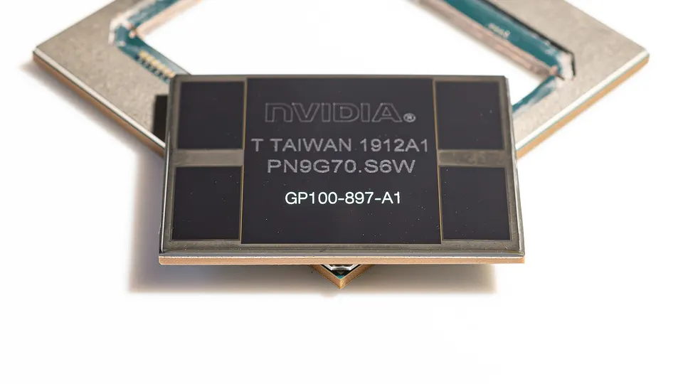
Interposer
A silicon base with fine wiring
Chips sit side by side on a silicon interposer whose wiring is far denser than a circuit board, linking GPU and HBM with thousands of short wires.
CoWoS-L
Bridges instead of one big slab
CoWoS-L embeds small silicon bridges in an organic base, so packages can grow to several reticle sizes without one giant, fragile silicon piece.
Size
Packages beyond the reticle
Today's packages already span several reticle areas. TSMC plans a 9.5-reticle version in 2027 that can hold 12 or more HBM stacks.
Update log
Tue 16 Jun
- Minor: PressPartnership
Wed 23 Apr 2025
- Minor: PressResearch
Thu 2 Jan 2025
- Minor: PressManufacturing
Fri 4 Oct 2024
- Minor: PressPartnership
Thu 15 Aug 2024
- Minor: PressManufacturing
About TSMC
TSMC
Chip foundry, N2, A16, CoWoS packaging
TSMC, founded in Taiwan in 1987, builds chips that other companies design. It makes most of the world's most advanced chips, including Apple's, NVIDIA's and AMD's. Its CoWoS packaging is a key bottleneck for AI chips.
- N2 (2 nm class) in volume production since Q4 2025. A16 is planned for the second half of 2026.
- Pledged $165B in total for US factories, packaging and R&D in Arizona.
- Makes nearly all leading AI chips and packages them with CoWoS.
- Founded
- 198739 yrs
- Headquarters
- Taiwan
- Status
- Public
- Listed
- TSM (opens google.com)NYSE
- Valuation
- public
- Staff
- ~83,825Dec 2024
- Works in
- ComputingChip factories (foundries)Manufacturing
- Coverage
- 3 programs · 17 updateslatest 16 Jun 2026checked 25 Sep
- Customers
- Apple (opens apple.com)NVIDIAAMD
- Suppliers
- ASML
- People
- C.C. Wei (opens en.wikipedia.org)Chairman and CEOMorris Chang (opens en.wikipedia.org)Founder (retired)