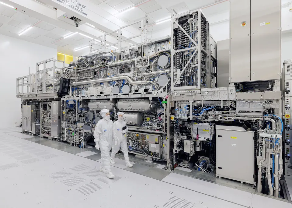

Milestones
- First EXE:5000 shipped to Intel21 Dec 2023Complete.
- First light and 10 nm lines in VeldhovenApr 2024Complete.
- ASML-imec High-NA lab opensJun 2024Complete.
- EXE:5200B production-grade tool shipped2025Complete.
- High-volume manufacturing insertion (Intel 14A)Target 2027Current milestone.
- Hyper-NA (~0.75 NA) feasibility decisionTarget 2030Not yet reached.
Most important updates
- 16 Dec 2025
- 2 Sep 2025
- Apr 2025
- Feb 2025
- 21 Dec 2023
Upcoming
- Q4 2026Intel 14A customer and High-NA volume decisions (next)
- 2027High-volume manufacturing insertion (Intel 14A)
- 2030Hyper-NA (~0.75 NA) feasibility decision
Current obstacles
- Thinner resists and depth of focusSharper optics have less focus depth, needing thinner light-sensitive coatings that are harder to make.
- Cost versus multi-patterningIt only wins if one High-NA pass is cheaper than 2 or more standard EUV passes.
Physics limits
- Resolution is set by wavelength and apertureThe finest printable line is about k1 × wavelength ÷ NA. With 13.5 nm light and NA 0.55, roughly 8 nm lines is the floor. Going further needs NA ~0.75, with even larger mirrors and steeper light angles.
- Depth of focus shrinks as NA growsFocus depth falls roughly with 1/NA², so High-NA images stay sharp over only a few tens of nanometres. Resists must be thinner, which absorbs less light and makes edges noisier.
- Too few photons per featureEach EUV photon carries about 92 eV, 14 times a deep-UV photon, so a given dose is made of few photons. Random counts per tiny feature cause rough edges and missing contacts (stochastic defects).
How it works
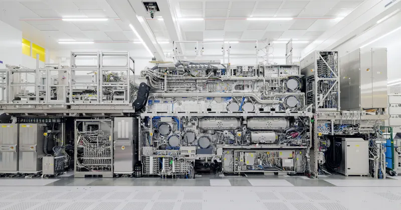
Source
Tin plasma light
The same laser-blasted tin plasma as standard EUV makes the 13.5 nm light.
Anamorphic
Different magnification per axis
The optics shrink the pattern 8x one way and 4x the other, to avoid steep angles on the mask.
Stitching
Half-field exposures
Each shot covers half the usual area, so the biggest chips need 2 shots stitched together.
Spec sheet
| Spec | High-NA EUV (EXE) | NXE:3800E (0.33 NA) | Change |
|---|---|---|---|
| Numerical aperture | 0.55R (reported) | 0.33 | ▲ 0.2 |
| Resolution | 8 nmR (reported) | 13 nm | ▼ 5 nm |
| Wavelength | 13.5 nmR (reported) | — | —no comparable change |
| Exposure field | 26 x 16.5 mm (half field)R (reported) | 26 x 33 mm | —no comparable change |
| Throughput (EXE:5200B) | >175 wafers/hourR (reported) | — | —no comparable change |
| System price | ~€350M+E (estimated) | — | —no comparable change |
R reported by the company · E our estimate
Papers & demos
- Jun 2024demoASML-imec High-NA EUV lab opens in Veldhoven (opens asml.com)Lets chipmakers and suppliers develop processes before machines reach factories.
- Apr 2024demoFirst 10 nm dense lines printed with High-NA EUVRecord fine lines for a production-class lithography machine.
Update log
Tue 16 Dec 2025
- Major: PressTest
Tue 2 Sep 2025
- Minor: BlogHardware
Apr 2025
- Minor: PressCommercial
Feb 2025
- Minor: PressTest
Wed 17 Apr 2024
- Minor: XTest
Thu 21 Dec 2023
- Major: XHardware
About ASML
ASML
EUV lithography machines
ASML, based in the Netherlands, is the only maker of EUV lithography machines, which every leading chip factory needs. They print circuit patterns with extreme-ultraviolet light. Its next generation, High-NA EUV, prints even finer lines.
- Only EUV supplier. A standard machine costs about €200M, a High-NA one about €350M or more.
- Shipped the first High-NA EUV machine to Intel in December 2023.
- Led Mistral AI's Series C with €1.3B in September 2025.
- Founded
- 198442 yrs
- Headquarters
- Netherlands
- Status
- Public
- Listed
- ASML (opens google.com)NASDAQ
- Valuation
- public
- Staff
- ~44,027Dec 2024
- Works in
- ComputingLithography machinesManufacturing
- Coverage
- 2 programs · 13 updateslatest 15 Jul 2026checked 25 Sep
- Partners
- Mistral AI
- Suppliers
- Carl Zeiss SMTTrumpf (opens trumpf.com)
- People
- Christophe Fouquet (opens asml.com)President and CEORoger Dassen (opens asml.com)CFO