

Milestones
- HBM3E 8-layer first supplied to customersMar 2024Complete.
- 12-layer HBM3E mass production25 Sep 2024Complete.
- HBM4 development completed, mass production readied11 Sep 2025Complete.
- HBM4 volume supply for NVIDIA RubinTarget 2026Current milestone.
Most important updates
- 10 Mar 2026
- 28 Jan 2026
- Jan 2026
- 11 Sep 2025
- 19 Mar 2025
Upcoming
- 2026HBM4 volume supply for NVIDIA Rubin (next)
Current obstacles
- Stacking yieldOne bad chip can ruin a whole 12-layer stack, so yields are hard to keep high.
Physics limits
- DRAM bits leak awayEach bit is a little charge on a tiny capacitor that leaks within milliseconds, so every cell is rewritten about every 32–64 ms. Shrinking the capacitor makes leakage worse, which slows density gains.
- Stacks are height-capped and trap heatThe HBM standard caps a stack at 775 µm, so 16 dies must be thinned to about 30 µm each. Heat from lower dies must pass up through the stack, and DRAM loses data faster when hot.
- Bandwidth is wires × speedHBM4 already uses 2,048 data wires per stack. More wires need finer bumps that are harder to bond; faster signalling costs more energy per bit.
How it works
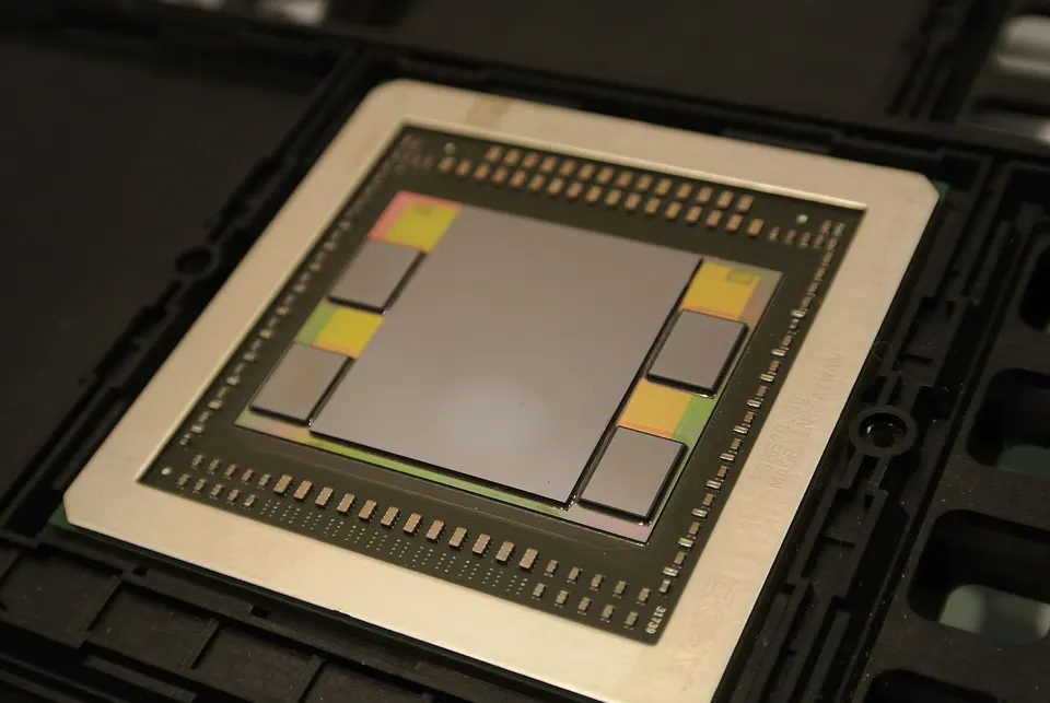
Stack
Memory chips in a tower
12 thin DRAM chips are stacked and linked by thousands of tiny vertical wires.
Width
Very wide connection
2,048 connections per stack let data flow to the AI chip much faster than normal memory.
Spec sheet
| Spec | HBM4 | HBM3E | Change |
|---|---|---|---|
| Interface width | 2,048 bitsR (reported) | 1,024 bits | ▲ 1,024 bits |
| Data rate per pin | Over 10 GbpsR (reported) | — | —no comparable change |
R reported by the company
Update log
Tue 10 Mar
- Minor: PressHardware
Wed 28 Jan
- Minor: PressCommercial
Jan 2026
- Minor: PressHardware
Thu 11 Sep 2025
- Major: PressHardware
Wed 19 Mar 2025
- Major: PressHardware
About SK hynix
SK hynix
HBM memory, DRAM, NAND
SK hynix is a South Korean memory chip maker and the leading supplier of high-bandwidth memory (HBM), the stacked memory placed next to AI chips. It is NVIDIA's main HBM supplier.
- First to supply HBM3E to customers (March 2024) and first to mass-produce 12-layer HBM3E (Sept 2024).
- Completed HBM4 development and readied mass production in September 2025.
- Main HBM supplier for NVIDIA's AI GPUs.
- Founded
- 198343 yrs
- Headquarters
- South Korea
- Status
- Publicof SK Group
- Listed
- 000660 (opens google.com)KRX
- Valuation
- public
- Works in
- ComputingPackaging & memory
- Coverage
- 1 program · 6 updateslatest 10 Mar 2026checked 25 Sep
- Customers
- NVIDIA
- Partners
- TSMC